Validation engineering is only a trap if you let it be

Throughout this subreddit and across the broader Semiconductor community, I noticed a lack of respect for Validation Engineering with many people claiming that once you start in it, you'll be stuck in it and hard to switch out.

But this is true for any job really where you get too complacent.

I've noticed that validation does have its fair share of perception challenges nowadays since it is mostly considered a cost center; you're at the tail end of the schedule, you generally don't have control over what is handed to you. Automation is also becoming prevalent in validation as well.

However, validation is, in my opinion, one of the best field for young engineers to start in and for people to experience another part of the design flow. You learn a bit about lab equipment and ensuring how data is considered good to hand off to key stakeholders. You engage with designers and other key members of the semi design flow. You also acquire an attitude of not looking down on validation people later in your career.

But nowadays, validation does tend to be very execution heavy and can leave you without a system level understanding of the chip you are testing and how it got there.

I say this because I've spent some time in validation after some time in other areas. Though I grumbled a bit while in it and people often looked down and to the right, I learned quite a bit of perspective I didn't have from other jobs.

Curious to hear your thoughts; do you think validation becoming increasingly perceived as lower on the totem pole?

reddit.com
▲ 5 r/chipdesign+1 crossposts

How bandgap references keep your personal electronics accurate when they heat up

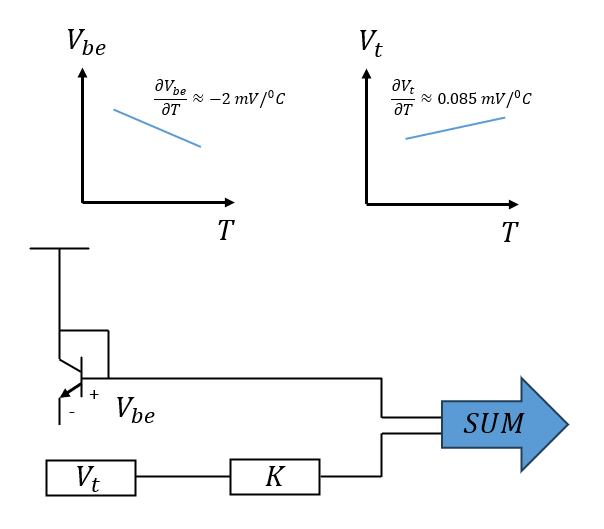
How PTAT and CTAT Voltages sum to cancel each other to generate a temperature-insensitive voltage

Why does your phone stay accurate when it heats up? Why don’t its analog bias points shift enough to break specs?

Because deep inside the chip there’s a tiny “reference” - the bandgap voltage reference (often ~1.2 V) - designed to stay stable across manufacturing variation, supply changes, and temperature.

A bandgap reference generates a stable voltage with low sensitivity to temperaturesupply, and process (often with trimming).

Most IC datasheets specify that the IC will work within a specific temperature range (such as -55 ̊ C to 125 ̊ C). Variations in temperature can shift bias points and thresholds enough to break specs without a stable reference and proper matching.

Bandgap references are found in virtually all analog circuits as stable references for high-precision analog functions, such as ADCs, DACs, and comparators. They are also used to bias current mirrors for setting bias points so that the resulting circuit is robust to PVT variations. Because of their ubiquity, they tend to be reused and modified depending on the fab process and the level of precision required.

Bandgaps look simple, but are a delicate balance of a few fundamental analog principles, including:

  • Matching: resistor ratios, BJT area ratios, amplifier offsets
  • Feedback: Forcing ΔV_BE and setting I_PTAT robustly
  • Temperature variation: How BJT and resistor characteristics vary over temperature, sometimes nonlinearly
  • Trim & Calibration: Output accuracy, temp trim, and curvature correction

Below is a self-biased bandgap design example I built that illustrates these principles.

Circuit Analysis

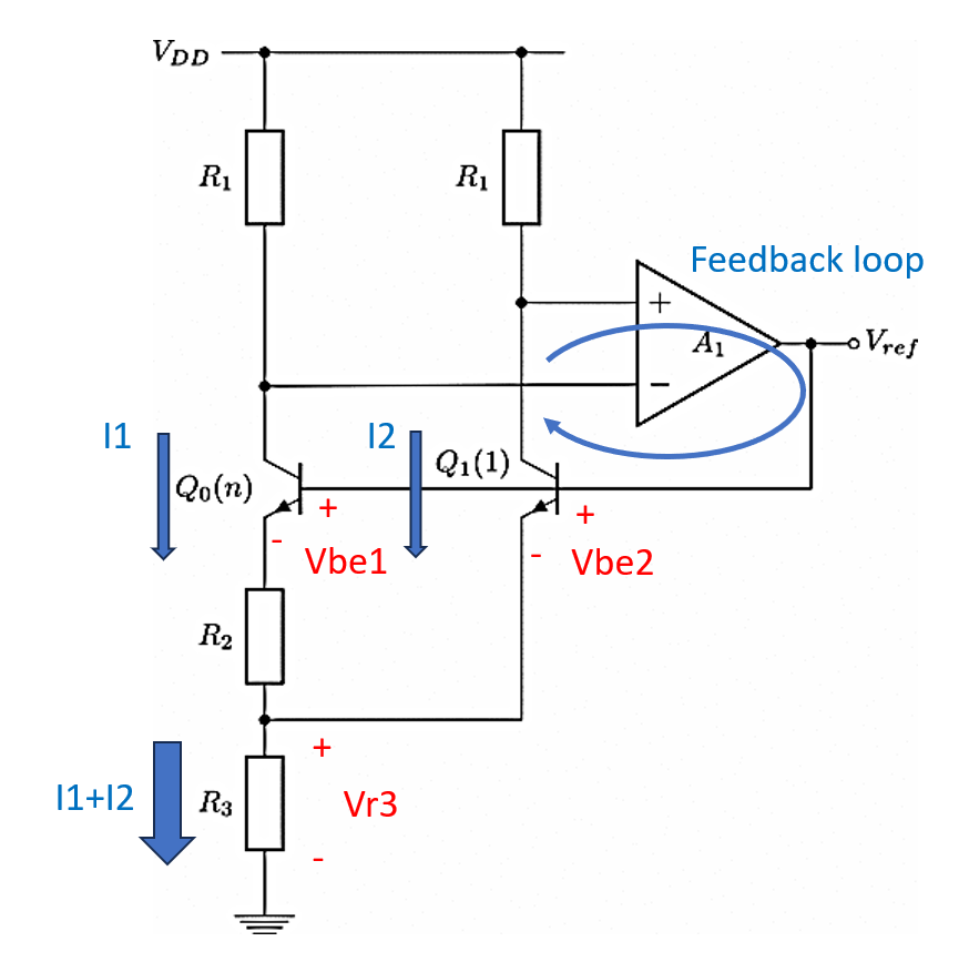
A Brokaw Bandgap Reference with key values labelled

Consider the Brokaw Bandgap reference in Fig. 1. The reference voltage is the output of the op amp. This circuit sums a PTAT voltage and a CTAT voltage:

  • A PTAT voltage (Proportional to absolute temperature) means that the voltage increases with increasing temperature.
    • The PTAT voltage is generated by the BJT base - emitter voltage difference ΔV_BE = Vt*ln(n) by forcing two BJTs to operate at different current densities (often via an emitter-area ratio n). This voltage appears across R3 in the above example.
  • A CTAT voltage (Complementary to absolute temperature) means that the voltage decreases with increasing temperature.
    • The CTAT voltage is generated across the base-emitter of the BJT which behaves like a diode. The reason behind this is related to the fact that the bandgap energy of silicon decreases with increasing temperature.

Additionally, the op-amp sets the PTAT current by driving the loop so its input nodes match (in the ideal case).

When both PTAT and CTAT voltages are summed with the right scaling, the first-order temperature dependence largely cancels, leaving a much flatter reference over temperature.

If you want to learn more, I dive more in more depth into the derivation of the output voltage. I also add a fun story at the end about a group of young designers who “competed” to build the best bandgap—an exercise you can try at your own work.
https://www.siliconcodesign.com/p/the-bandgap-reference-a-primer

reddit.com
u/thesiliconmachine123 — 4 days ago

How Jitter degrades BER in High-Speed Signal Integrity

Simplistic Overview for how Channel Loss and Jitter affect BER

Jitter is defined as the time variation in when a signal edge actually transitions compared to its ideal transition point. Jitter is a significant limiter of performance in high-speed applications because it affects how much of a time ”window” you have to accurately sample the digital data.

Jitter is broadly broken down into two major categories: Random and Deterministic:

Random Jitter comes from noise-like mechanisms that are fundamentally statistical in nature, such as thermal noise.

This is always uncorrelated and typically modelled as a Gaussian distribution due to the central limit theorem that states that summing up a variety of PDFs from uncorrelated sources tend toward a Gaussian distribution.

Deterministic Jitter is jitter from repeatable structure in the system such as data movement and reflections.

This jitter is typically bounded with a max and min timing shift - the edge shifts in a repeatable way. It can also be correlated or uncorrelated. Examples include:

  • Data dependent jitter (ISI) - Symbols from previous transitions spill into the next time window
  • Periodic Jitter
  • Bounded uncorrelated jitter

As link complexity has grown, many other jitter sources must be accounted for during design and measured in silicon.

How Channel loss and Jitter degrade Bit Error Rate

Both losses distort the signal in complementary ways:

  • Channel loss distorts the waveform itself by attenuating and smearing its higher-frequency content
  • Jitter introduces uncertainty in when transitions occur.

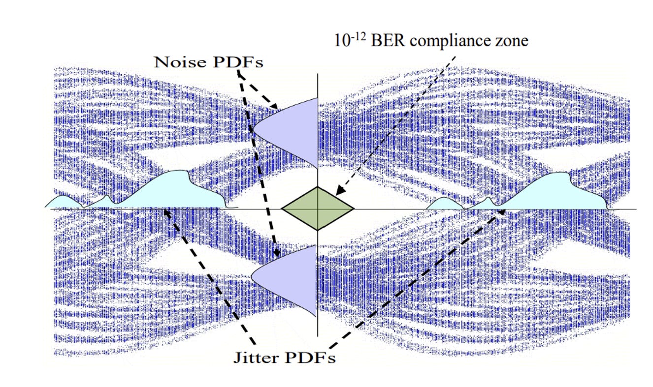
Together, these (and other effects such as reflections) reduce eye opening and increase the Bit error rate (BER) at your sampling edge.

A typical eye diagram showing both the effect of channel loss (rounding) and jitter (signal amplitude and timing uncertainty). Source: M. Li. “Design and Verification for High-Speed I/Os at 10 to 112 to 224 Gbps, and 448 Gbps with Jitter, Signal Integrity, and Power Optimized: A Tutorial for Designcon 2026” DesignCon 2026

Bit error rate is not easy to measure directly because of the amount of time it takes to observe enough samples (sometimes trillions) to get a statically significant measurement of BER. It is usually easy to measure a BER of 10^-6 which is 1 error in 1 million bits with a BERT (Bit error rate tester), but some systems require BERs of 10^-12 which is one error in one-trillion bits!

How Jitter components and BER are related

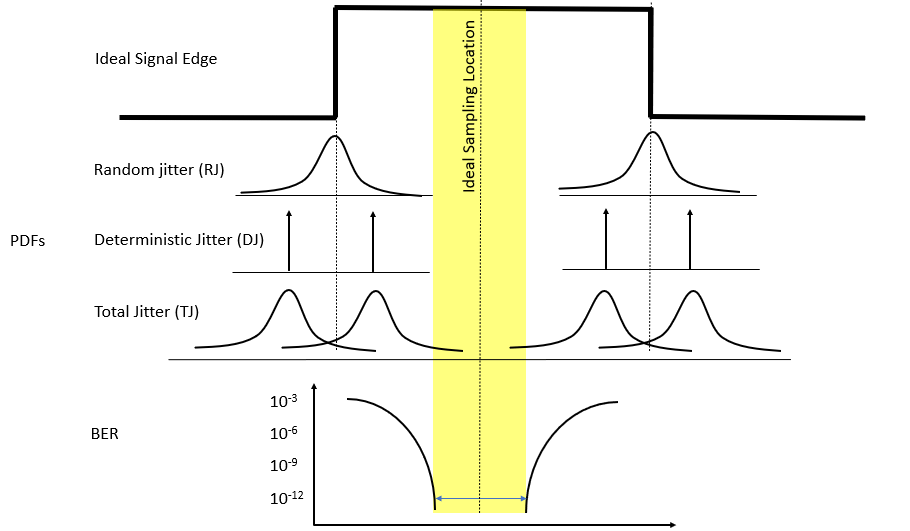
Often, lower BERs are often extrapolated from higher BER curves. The Dual-Dirac model is a widely accepted “worst case model” used to extrapolate this. To show how BER is driven from jitter, consider the two major classes of jitter:

  • RJ spreads the signal edge according to a Gaussian distribution
  • DJ shifts the signal edge with two “bounds”. In this model, the worst cases are represented as two worst case impulse ”spikes” at either bound. (Note that this is not the actual PDF of the DJ as it varies in uniformity within the bounds. However, this works fine because we only care about the “tails” of the RJ curve convolved at the bounds)

These two sources combine in a “convolution” format, so the gaussians of the RJ map onto the bounds of the DJ to obtain the Total Jitter (TJ). The BER is then estimated from the tails of the total-jitter distribution: as the distribution spreads further into the sampling margin, the probability of error increases.

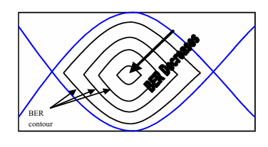
You can then use this to map contours of constant BER in the center of the eye that decrease the more the signal is sampled at the center of the eye:

Contours of constant BER. Source: M. Li. “Design and Verification for High-Speed I/Os at 10 to 112 to 224 Gbps, and 448 Gbps with Jitter, Signal Integrity, and Power Optimized: A Tutorial for Designcon 2026” DesignCon 2026

The above is an excerpt from my post "High-Speed Signal Integrity: Physical Impairments and Equalization Architectures" where I discuss related information such as channel loss, PAM-4, and DSP-based architectures. For full context and more detailed information, check out the full post at the following link: https://www.siliconcodesign.com/p/signal-integrity-a-primer

reddit.com
u/thesiliconmachine123 — 6 days ago
▲ 113 r/Semiconductors+1 crossposts

AI has made the lives of chip designers harder, not easier

AI is EDA is not as effective as pundits claim it to be, for now. Artour Levin, CVP AI Silicon Engineering, Microsoft, “EDA Opportunities in building high performance AI accelerators” DAC 2026

I made this startling conclusion after attending the Design Automation Conference, the heart of design automation for chips, and synthesizing my findings.

There, I noticed that most experienced silicon engineers do not completely trust AI to design chips quite yet.

On the design side, AI does offer some productivity and quality of life benefits for chip designers, such as vibe coding RTL.

However, quite paradoxically, silicon for AI applications requires increasingly complex architectures and compute requirements. These introduces several challenges chip designers have to deal with, including:

- More complex verification, which has historically been the most labor-intensive step in chip design

- Multiphysics challenges with off-chip thermal/SI/PI/packaging  

- Late-stage firefighting in power closure due to bursty, unpredictable LLM workloads in systolic arrays

What are your thoughts? Have you seen AI improve the chip design flow, or is it simply another frustrating flow to pick up?

Edit: added the photo at the top

Edit: I enjoy seeing the interesting discussion this sparked. For context, I attended DAC all four days out of my own pocket, sat in panels, took diligent notes, and shot that photo myself to pull this writeup together. I appreciate those who engaged thoughtfully and acknowledged AI definitely offers tangible quality-of-life enhancements for designers today, but is nowhere near autonomously running full flows yet.

reddit.com
u/thesiliconmachine123 — 7 days ago
▲ 0 r/chipdesign+1 crossposts

Analog Design is Taught Inefficiently - and what to do about it

Analog design is one of the hardest yet inefficiently taught subjects among Electrical Engineering Specialties.

Analog design is difficult to self teach for two reasons: the complexity of the material, and the intuition gained through Cadence simulation is not easy to access outside of a job.

One of the best ways to understand complex subjects such as analog design is to break down the complexity into bite size pieces and rephrase in words you understand.

However, it can be difficult to know where to start from or even how to self-teach. Most people were actually never taught how to self teach complex subjects. Self teaching requires a discipline and willingness to do what Cal Newport refers to as "Deep Work".

These are the tips I have for anyone trying to self study analog design:
💠 Pick one foundational book or course and read/take it (such as Razavi for Analog design, Andrew Ng for AI)
💠 For each chapter or section, write a bottom-up principle of operation summary in your own words where you describe how a specific circuit works step for step
💠 After reading the book / taking the course, create an architectural top-down map of the different topologies for each block and the pros/cons of each
💠 Layer on more complex and common blocks from simpler ones (such as folded cascode OTAs)

I find that self teaching is a very slow and cumbersome process - at first. However, it does get easier over time as concepts start clicking and you don't expend mental bandwidth figuring out what prerequisite knowledge you need to know.

I go more into depth in the above process in my post, "Learn Analog Mixed Signal Design the Efficient Way", along with links to several block level and architecture level deep dives throughout.

https://chadw.substack.com/p/learning-analog-design-the-efficient?r=23t7yt

u/thesiliconmachine123 — 2 months ago
▲ 10 r/chipdesign+1 crossposts

High-Speed Signal Integrity: Physical Impairments and Equalization Architectures

At 112Gbps and 224Gbps, a copper PCB trace stops acting like a simple conductor and begins behaving like a low-pass filter. It aggressively attenuates high frequencies, rounding out the sharp edges of digital pulses until the eye diagram completely collapses.

Signal Integrity isn't a passive list of textbook definitions—it is an active, multi-variable battle between physical channel impairments and silicon architecture.
To meet Bit Error Rate (BER) specifications, hardware teams cannot look at components in isolation. You have to understand the exact mathematical friction between channel loss, random clock jitter distributions, and the digital equalization loops (FFE, CTLE, and DFE) engineered to reverse them.

In this deep dive, I bypass the standard glossary-level summaries to map out the physics of high-speed signal degradation and the architectural boundaries of modern transceiver DSP networks.

Read the complete analysis on Inside the Silicon Machine:

https://chadw.substack.com/p/signal-integrity-a-primer

u/thesiliconmachine123 — 3 months ago